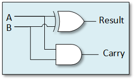
A half adder is a circuit that receives two 1-bit inputs and adds them together to generate a 1-bit result output and a 1-bit carry. The basic building blocks (gates) of a half adder consist of an
XOR gate and an
AND gate. The below truth table and Kmap shows you again how these gates were chosen.
As usual, we always start the design process by creating a truth table, showing all possible input combinations and writing down the expected output states.
 |
| Truth Table for Half Adder (Fig 2) |
After you create the truth table, draw the Kmap for each output as shown in Fig. 3:
 |
| Fig 3 |
Author’s Tip: It is important to understand how these basic building blocks are used together just in case you are asked. It is too easy as a RTL designer to just type in Verilog: R = A + B; Now you will have better understanding of what’s happening during synthesis.
|
This was just one question of over 50 questions that are in the Digital Logic RTL & Verilog Interview Questions Book. The book contains 41figures and drawings, and 28 pratical Verilog code examples.
 |
| Digital Logic RTL & Verilog Interview Questions |
You can purchase the Paperback book on
Amazon or purchase the PDF E-Book version directly from us on our
purchase page.


0 Comments